Semiconductor Tool Manufacturer

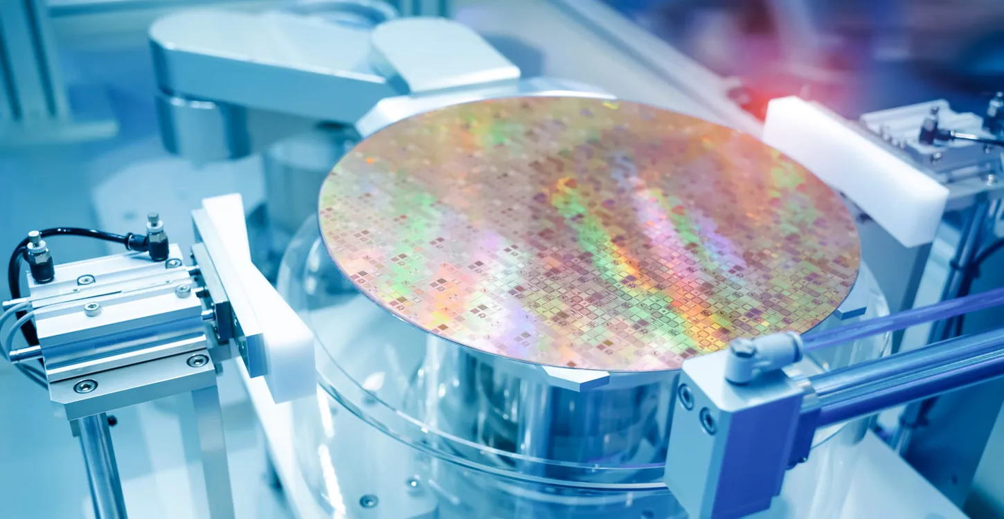
The semiconductor industry is comprised of the design, manufacturing, assembly, and test of integrated circuits for use in data processing, communications, consumer electronics, automotive, and aerospace. Semiconductor tool manufacturers develop and sell semiconductor wafer tools for the fabrication of microelectronic components. They typically consist of multiple wafer processing stations placed around a central, automated handling unit. As chips become more complex, greater levels of automation are necessary in order to lower costs, increase productivity, and improve process reliability and product quality.
All semiconductor tools consist of three components or groups of components: a number of process/cleaning/cooling chambers, chambers for loading and unloading, and multiple robots for transferring wafers between chambers. Each chamber operates at different pressures with different process gases or plasma, all which must be carefully controlled.
The leading sensor developer for state of the art technology, INFICON offers a vast portfolio of sensors to serve thousands of process monitoring applications for semiconductor manufacturing tools. Our core technologies include mass spectrometry, quartz crystal microbalance, RF DC detectors, optical sensors, vacuum gauges and leak detectors.
INFICON products are proven to increase productivity, efficiency, uptime and yield, ensuring that original equipment manufacturers (OEMs) can successfully sell equipment to meet growing semiconductor needs.
Submarkets
In the manufacturing process of integrated circuit (IC), electronic circuits with components such as transistors are formed on the surface of a silicon crystal wafer. Several steps of different processes like deposition, photoresist coating, lithography, etch or ion implantation are necessary. These applications span a range of pressures, ambient gases and plasma processing and require precise gas composition control and actively monitored chamber cleanliness. INFICON provides latest and innovative technology of vacuum, mass spectrometry, RF and QCM sensors to tool manufacturers, tailored to specific and leading-edge applicationsto increase process quality and tool up time.
The silicon wafer manufacturing process can be divided into two stages, namely, pulling single crystal ingots (CZ Method), and slicing and polishing the silicon wafers.
With the pulling of single crystal silicon method, polycrystaline silicon nuggets are placed in a quartz crucible, which is set in a graphite crucible surrounded by graphite heaters in the crystal pulling chamber. These nuggets are melted by heating in an Argon atmosphere under vacuum and then pulled slowly using a seed crystal. For vacuum pressure control and vacuum chamber integrity, our vacuum gauges and leak detectors guarantee high production output and product quality.
Metrology and inspection are important for the management of the semiconductor manufacturing process. There are 400 to 600 steps in the overall manufacturing process of semiconductor wafers, which are undertaken in the course of one to two months. If any defects occur early on in the process, all the work undertaken in the subsequent time-consuming steps will be wasted. Metrology and inspection processes are therefore established at critical points of semiconductor manufacturing process to ensure that a certain yield can be confirmed and maintained.
The most comprehensive and advanced Process Control and Maintenance Management Software Suite for the electronics manufacturing industry is available from INFICON. Our solutions are proven to increase capital productivity, labor efficiency and overall factory efficiency by detecting and predicting excursions, automating complex decision making, and delivering industry-leading process control capability. Collect the Right Information - Analyze the Right Data - Make the Right Decisions.
Wafer Dicing is a back end semiconductor manufacturing process the completed wafer is sliced into individual chips. Automated methods include mechanical sawing and laser cutting. Mechanical sawing is accomplished with a dicing saw that uses a circular dicing blade to cut the die into sizes ranging from 35mm to 0.1mm. Die-handling equipment is then used to transfer the chips to the die-bonding process. Individual die are too small and delicate to be handled on their own. They need to be protected while also being electronically tested in a safe and efficient way. Die Bond, also called Die Attach, is the process of securing the bare die to a substrate. In later steps the substrate will act as the interface between the microscopic scale of the chip and the macroscopic scale of electronics manufacturing. It will also be the foundation of the protective chip package seen on PC boards. After die bond, the wire bond process connects each pad on the die to a corresponding pad on the substrate via a thin gold wire. This forms the electrical connection between the silicon die inside the chip package and the pins on the outside. The wire bond process is used on classic chip packages such as dual in-line package or DIP, with the familiar black oblong rectangle with silver pins sticking out like bug legs, as well as PLCC packages with conductors on all four sides. A modern alternative to wire bonding, flip chips are mounted "upside-down". Hence the name "flip chip". Instead of wires connected around the periphery of the chip as in wire bonding, an array of "bumps" are formed on the surface of the chip. These bumps are then used as connection points from the chip to the outer package.
The advantages of flip chip technology include:
- Better connections to the chip as opposed to wire bonding where the wires add extra length, capacitance and inductance that limit signal speed.
- Wrapping up the back end semiconductor manufacturing process the bonded die and frame are sealed - either by a molded plastic compound, or by the attachment of a sealed lid. The silicon die is now ready to be used in electronics manufacturing.
- Due size reduction and increasing output requirements vacuum typically used to improve back end processes. For vacuum pressure control and vacuum chamber integrity INFICON vacuum gauges and leak detectors guarantee high production output and product quality.
The entire process of creating a silicon wafer with working chips consists of thousands of steps and can take more than three months from design to production. To get the chips out of the wafer, it is sliced and diced with a diamond saw into individual chips. Cut from a 300-mm wafer, the size most often used in semiconductor manufacturing, these so-called 'dies' differ in size for various chips. Some wafers can contain thousands of chips, while others contain just a few dozen.
The chip die is then placed onto a 'substrate'. This is a type of baseboard for the microchip die that uses metal foils to direct the input and output signals of a chip to other parts of a system. And to close the lid, a 'heat spreader' is placed on top. This heat spreader is a small, flat metal protective container holding a cooling solution that ensures the microchip stays cool during operation.
Let's work closely to address your specific needs
We are excited to work alongside you at the Semiconductor Innovation Center, where our expertise, solutions, and customer service come together to drive success in the semiconductor industry.


